
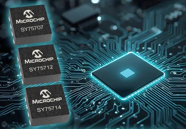

September 14, 2026 / SemiMedia / — Microchip Technology has introduced the SY757xx family of 1.2V-output LVCMOS clock buffers for next-generation FPGA, SoC and CPU platforms, providing single-chip clock distribution and voltage translation across different board voltage levels.
The SY757xx family supports frequencies from 0 Hz to 250 MHz and voltage translation across a 1.2V to 3.3V input range, including configurations that connect 3.3V components directly to FPGAs and SoCs requiring 1.2V clock signals. Additive jitter is as low as 26 femtoseconds.
Microchip said lower I/O voltages in advanced FPGAs, SoCs and AI accelerators are making traditional discrete clock translation more difficult. Discrete voltage-divider implementations can increase component count and affect duty-cycle accuracy and signal integrity, while the SY757xx devices combine level translation and clock fanout in a single device.
The family offers multiple single-ended and differential input configurations with different LVCMOS output options. Target applications include AI and machine learning acceleration, embedded vision, industrial control, IoT, networking and communications, and other systems requiring low latency and accurate clock distribution.
Three devices — the SY75707TWL-TR, SY75712TWL-TR and SY75714TWL-TR — are now in volume production, while eight additional SY757xx family members are sampling in limited quantities. Production devices are offered in compact 8-pin VDFN or TDFN packages.
Pricing for the production devices ranges from $0.50 to $0.83 per unit depending on configuration in quantities of 10,000.






All Comments (0)