
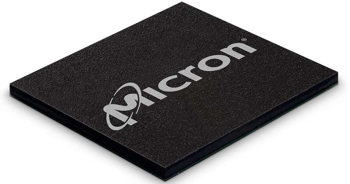

October 26, 2026 / SemiMedia / — Micron plans to ramp its next-generation G11 3D NAND in the second half of 2027, targeting approximately twice the bit density of G9, up to 50% faster I/O and more than 25% lower data-transfer energy per bit. The company outlined the technology at its October 21 webinar.
G11 will combine more than 400 layers with wafer-on-wafer bonding. Manufacturing the memory array and peripheral logic separately before bonding them together allows each to use processes optimized for its requirements, supporting improvements in density, interface performance and efficiency.
President and Chief Technology and Products Officer Scott DeBoer said Micron considers the timing right to introduce wafer bonding based on its cost and the capabilities required by upcoming products. The company has not disclosed the exact word-line count or number of stacking decks and expects to provide further details closer to the 2027 ramp.
Density gains will come from both additional layers and tighter memory-cell pitch. These advances could support higher-capacity SSDs and faster data movement, although NAND-level improvements do not translate directly into equivalent gains in complete SSD performance or power consumption.
Beyond G11, Micron is developing high-mobility materials, denser cell architectures and more energy-efficient devices and data paths. Its roadmap combines smaller lateral cell dimensions with increased vertical stacking. Specifications and production schedules for those later generations remain undisclosed.



All Comments (0)