

September 9, 2026 / SemiMedia / — Samsung Electronics has opened its Advanced Package Lab in Yokohama, Japan, as part of a ¥40 billion investment aimed at accelerating advanced packaging development for AI chips and strengthening cooperation with Japanese semiconductor materials, components and equipment suppliers.
The facility, located in Yokohama's Minato Mirai district, covers about 6,600 square meters. Samsung plans to invest approximately ¥40 billion over five years from 2024, with Japan's Ministry of Economy, Trade and Industry providing ¥22.5 billion in support.
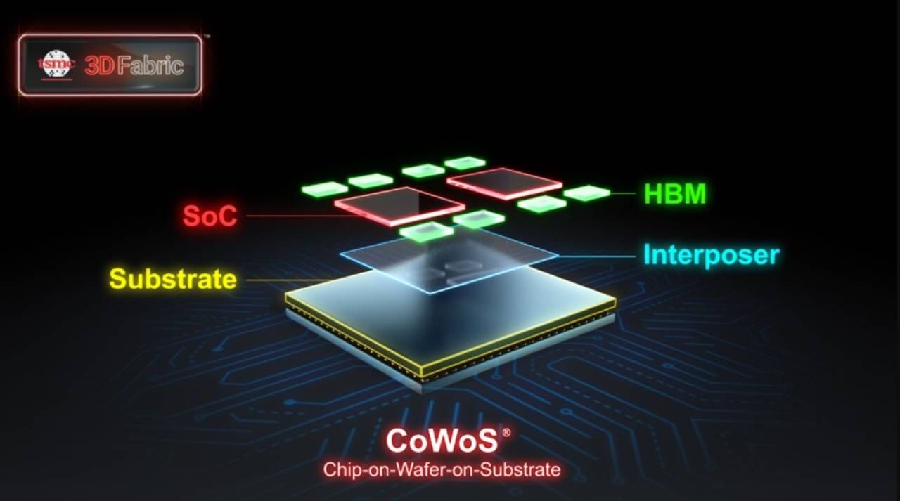
As AI data center demand increases, advanced packaging is becoming more important for efficiently connecting high-bandwidth memory, GPUs and other high-performance chips. Japan has a strong position in semiconductor back-end materials and equipment, and Samsung currently works with more than 50 Japanese companies on AI chip packaging processes.
Japanese suppliers including Sumitomo Bakelite, Resonac and Mitsubishi Gas Chemical hold important positions in packaging and substrate materials, making local cooperation increasingly relevant as packaging complexity rises.
The Yokohama center is also expected to shorten material evaluation and development cycles. New materials developed by Japanese suppliers previously had to be shipped to South Korea for testing, with chemical approvals and import-export procedures sometimes adding as much as two months to the process.
With the new lab, Samsung can conduct material evaluation and prototype development in Japan before transferring selected technologies to its mass-production lines in South Korea.
Samsung plans to use the facility as a global R&D base for next-generation packaging, combining its semiconductor design and manufacturing capabilities with Japan's materials and equipment ecosystem to accelerate development for HBM, GPUs and other AI-related chips.




All Comments (0)