June 17, 2026 /SemiMedia/ — Samsung Electronics said researchers at its semiconductor R&D center have developed a three-dimensional stacked transistor structure with a 42nm gate pitch, marking a potential step forward for future logic semiconductor scaling.
The research was recently recognized with the Best Paper Award at the 2026 VLSI Symposium in Kyoto, Japan.
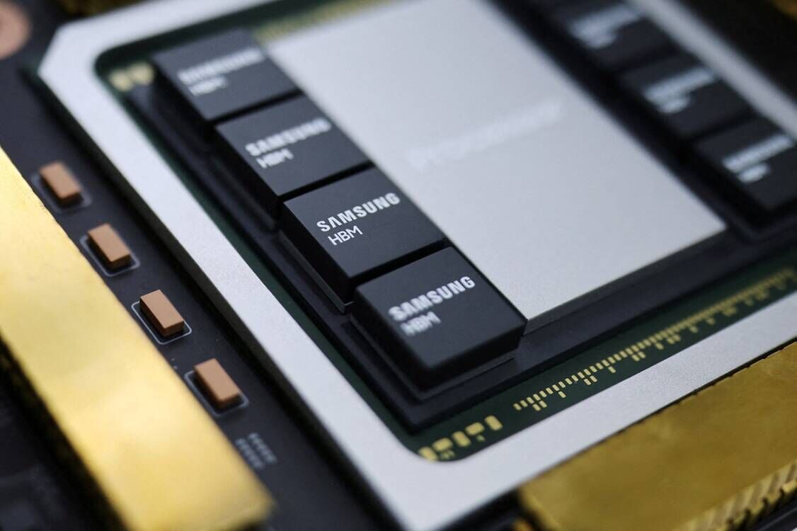
The development is significant because it extends the vertical stacking concept, already widely used in memory semiconductors, into logic chip architecture. Samsung previously used vertical stacking to increase NAND Flash density through V-NAND, while high-bandwidth memory has become a critical technology for the AI era.
Conventional logic semiconductors increase transistor density by placing devices side by side on a flat plane. However, as transistor spacing continues to shrink, thinner insulating layers and electromagnetic interference make further two-dimensional scaling increasingly difficult.
Samsung’s researchers addressed this challenge by stacking transistors vertically. The team achieved a 42nm gate pitch, narrower than the current industry level of about 48nm, and also introduced a structure that directly connects upper and lower transistors.
According to Samsung researchers, vertical stacking can allow more transistors to be placed within the same chip area, supporting smaller, lower-power and higher-performance semiconductors for artificial intelligence and high-performance computing applications.
As AI accelerators, server CPUs and advanced logic chips require greater compute density and energy efficiency, chipmakers are searching for new device structures beyond conventional planar scaling. Samsung’s 3D stacked transistor research could become one of the directions for future advanced logic technology.


All Comments (0)