
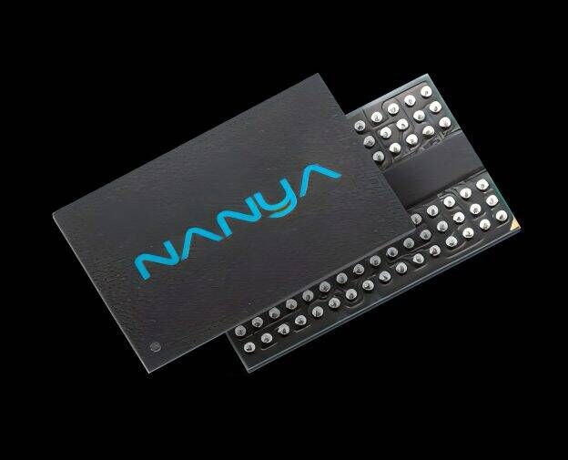

August 6, 2026 / SemiMedia / — Nanya Technology has announced additional capital investment to accelerate construction of its 5A fab, the company’s fifth 12-inch wafer manufacturing facility.
The company’s board has approved an increase in its 2026 capital expenditure from the previously planned NT$52 billion to NT$69.7 billion, representing an increase of approximately 34%.
Nanya Technology also plans to invest up to NT$346.6 billion between 2026 and 2029 in the construction of the 5A fab, advanced-process development and related equipment purchases.
The project represents the largest single investment in Nanya Technology’s history and one of the larger DRAM capacity-expansion plans in Taiwan in nearly two decades.
The investment will primarily support 10nm-class DRAM process technology, construction of the 5A fab, research and development and other general capital expenditures.
The new fab is expected to introduce extreme ultraviolet lithography equipment and serve as a major production base for Nanya Technology’s next-generation DRAM processes.
Total investment in the facility is estimated at approximately US$16 billion. The fab will gradually introduce the company’s advanced 1B, 1C, 1D and 1E 10nm-class DRAM processes.
The first phase is designed to reach a monthly wafer capacity of 35,900 units, while the facility’s planned maximum capacity is approximately 45,000 wafers per month.
Wafer production is scheduled to begin in the second half of 2027. Monthly capacity is expected to reach 30,000 wafers in 2028 and increase to 35,900 wafers in 2029.
Nanya Technology said funding for the 5A fab will come from internal resources, bank loans or other financing channels.
As demand for memory used in AI servers and data centers continues to grow, global DRAM manufacturers are expanding production capacity. Nanya Technology’s latest investment will accelerate its deployment of advanced DRAM processes and additional manufacturing capacity.





All Comments (0)