
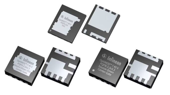

November 11, 2026 / SemiMedia / — Infineon has introduced its switching optimized OptiMOS 7 40 V power MOSFET portfolio for high frequency DC-DC conversion in AI servers, data centers and telecom infrastructure. The devices target designs that need higher efficiency and power density within limited board space.
Applications include the low voltage secondary stages of high voltage intermediate bus converters in emerging 800 V DC architectures, as well as intermediate bus converters in 48 V systems. Switching frequencies above 1 MHz are supported in suitable topologies. The devices are optimized for 5 V gate drive, support gate driver ecosystems used with GaN, and have a maximum junction temperature of 175°C.
Infineon balances on-resistance, output charge and gate charge to address conduction and switching losses. Comparing the source-down IQE010N04LM7CGSC with the OptiMOS 6 IQE013N04LM6CGSC, the company reports up to 33% lower maximum on-resistance at a gate-source voltage of 4.5 V. The output charge and gate charge figures of merit each improve by up to 35%.
The IQE010N04LM7CG and IQE010N04LM7CGSC use 3.3 mm × 3.3 mm PQFN source-down center-gate packages, with overmolded and dual-side cooling options. Both specify maximum on-resistance of 1.0 mΩ at a gate-source voltage of 10 V. For the IQE010N04LM7CGSC, the datasheet specifies 1.3 mΩ maximum at 4.5 V, measured at a junction temperature of 25°C and drain current of 20 A.
The larger 5 mm × 6 mm PQFN drain-down packages support dual-side cooling. The ISCH65N04LM7SC, ISCH69N04LM7SC and ISC011N04LM7SC specify maximum on-resistance of 0.65 mΩ, 0.69 mΩ and 1.1 mΩ, respectively, at a gate-source voltage of 10 V.
For thermal design, the IQE010N04LM7CGSC datasheet gives maximum junction-to-case thermal resistance of 1.0°C/W through the bottom and 1.4°C/W through the top, providing two heat removal paths for compact power stages.
The OptiMOS 7 40 V switching optimized portfolio is available and in mass production.








All Comments (0)