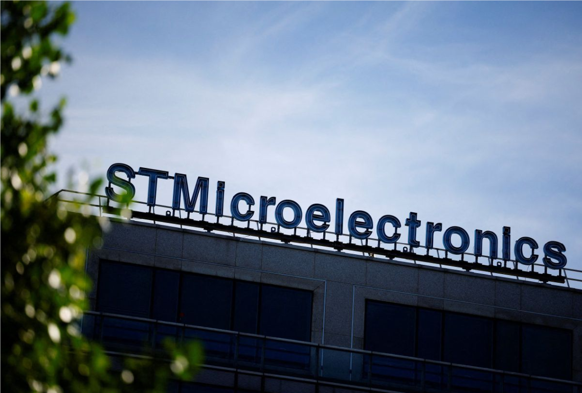
September 18, 2025 /SemiMedia/ — STMicroelectronics said it will invest $60 million in its Tours, France site to build a pilot line for advanced semiconductor manufacturing, with operations expected to begin in the third quarter of 2026.
The project will focus on panel-level packaging (PLP), a technology that shifts chip production from small round wafers to larger square panels, improving throughput and automation. PLP reduces reliance on traditional assembly steps often carried out in Asia, making it more cost-efficient to produce advanced chips in Europe.
STMicroelectronics, one of Europe’s largest chipmakers, has been restructuring its European footprint by phasing out older production lines and redefining the role of factories in France and Italy. The Tours site will play a central role in implementing the company’s long-term strategy for advanced packaging.
The company has already deployed PLP technology at its Muar, Malaysia plant, producing more than five million chips per day for a customer. The new investment in France aims to bring this capability closer to European markets, strengthening STMicroelectronics’ position in the global semiconductor supply chain.


All Comments (0)