August 15, 2025 /SemiMedia/ — Samsung Electronics plans to invest 25 billion yen (about $170 million) to establish an advanced chip packaging research and development center in Yokohama, Japan, scheduled to begin operations in March 2027. The move is aimed at strengthening Samsung’s position in the high-risk packaging market and intensifying competition with TSMC.
The center will collaborate with Japanese semiconductor materials and equipment suppliers, including Disco, Namics, and Rasonac, while also expanding research partnerships with the University of Tokyo. Samsung intends to recruit a large number of master’s and doctoral-level researchers to support the facility, which will receive a 2.5 billion yen subsidy from the city of Yokohama.
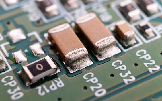
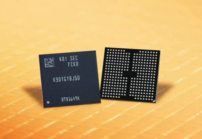
The new R&D hub is located in the Leaf Minato Mirai building near Yokohama Port, covering 47,710 square meters across 12 floors above ground and 4 underground, housing both the laboratory and a pilot production line. Samsung aims to advance packaging technologies that integrate GPUs, high-bandwidth memory (HBM), and other storage chips into a single module, critical for AI chip performance without requiring extreme miniaturization.
Packaging is central to Samsung’s turnkey manufacturing services, which combine wafer fabrication and packaging, an area where TSMC has long held a technological edge. TSMC established a related research facility at the University of Tokyo in 2019 to advance packaging techniques.
Japan hosts a number of key materials and equipment suppliers, including Rasonac and Namics in bonding films, Uemura for gold plating in packaging, Disco for cutting equipment, and MEC for adhesives and surface treatment materials.
According to Counterpoint Research, the advanced chip packaging market is projected to grow from $34.5 billion in 2023 to $80 billion by 2032. TSMC, Intel, and ASE are leading players, while Samsung holds a 5.9% market share, still trailing in 2.5D and 3D packaging technologies. Nevertheless, Samsung recently secured a $16.5 billion contract to manufacture Tesla’s next-generation AI6 chips, highlighting its growing turnkey service capabilities.


All Comments (0)