
SemiMedia SemiMedia
  • Breaking News
  • MarketWatch
  • Distribution
  • Manufacturer
  • Video
  • About us
Home › MarketWatch › SEMI: Global semiconductor packaging materials market to reach $29.8 billion by 2027
  • 0

SEMI: Global semiconductor packaging materials market to reach $29.8 billion by 2027

SemiMediaEdit
May 25, 2023

May. 25, 2023 /SemiMedia/ -- According to the Global Semiconductor Packaging Materials Outlook report jointly released by SEMI, TECHCET and TechSearch International, driven by strong demand for new electronic innovations, the global semiconductor packaging materials market is expected to reach US$29.8 billion by 2027, with a compound annual growth rate (CAGR) of 2.7%, up from $26.1 billion in revenue in 2022
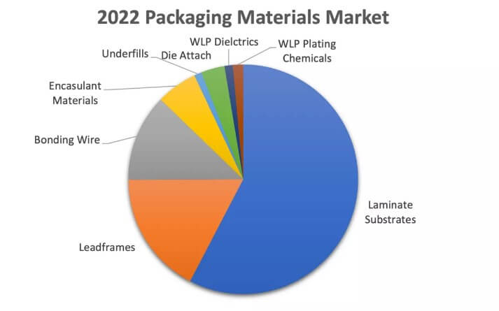
SEMI: Global semiconductor packaging materials market to reach $29.8 billion by 2027-SemiMedia

High-performance applications, 5G, artificial intelligence (AI) and the adoption of heterogeneous integration and system-in-package (SiP) technologies are increasing demand for advanced packaging solutions. The development of new materials and processes to enable chips with higher transistor density and greater reliability are also contributing to market growth.

“The semiconductor packaging materials industry is undergoing significant changes as new technologies and applications are driving demand for more advanced and diverse materials,” said Jan Vardaman, President and founder of TechSearch International. “Advances in dielectric materials and underfill are driving strong demand for fan-in and fan-out wafer level packaging (FOWLP), flip chip, and 2.5D/3D packaging. New substrate technologies such as silicon interposers and organic interposers using RDL (Re-Distribution Layer) are also key growth drivers of packaging solutions. At the same time, research on laminate substrates with finer features continues with the development of glass cores for build-up substrates.”
Related

electronic components news Electronic components supplier Electronic parts supplier SEMI Semiconductor Packaging Materials TECHCET TechSearch International
Kyocera to invest $2.9 billion to develop cutting-edge chip components in AI and other fields
Previous
Malaysia aims to account for 15% of the global semiconductor market by 2030
Next

All Comments (0)

Back
No Comment.

Top Post

Mouser Electronics expands to the Philippines with local customer service center
Qualcomm ranked first in the world's top ten IC design companies
Fire broke out at AKM factory in Japan
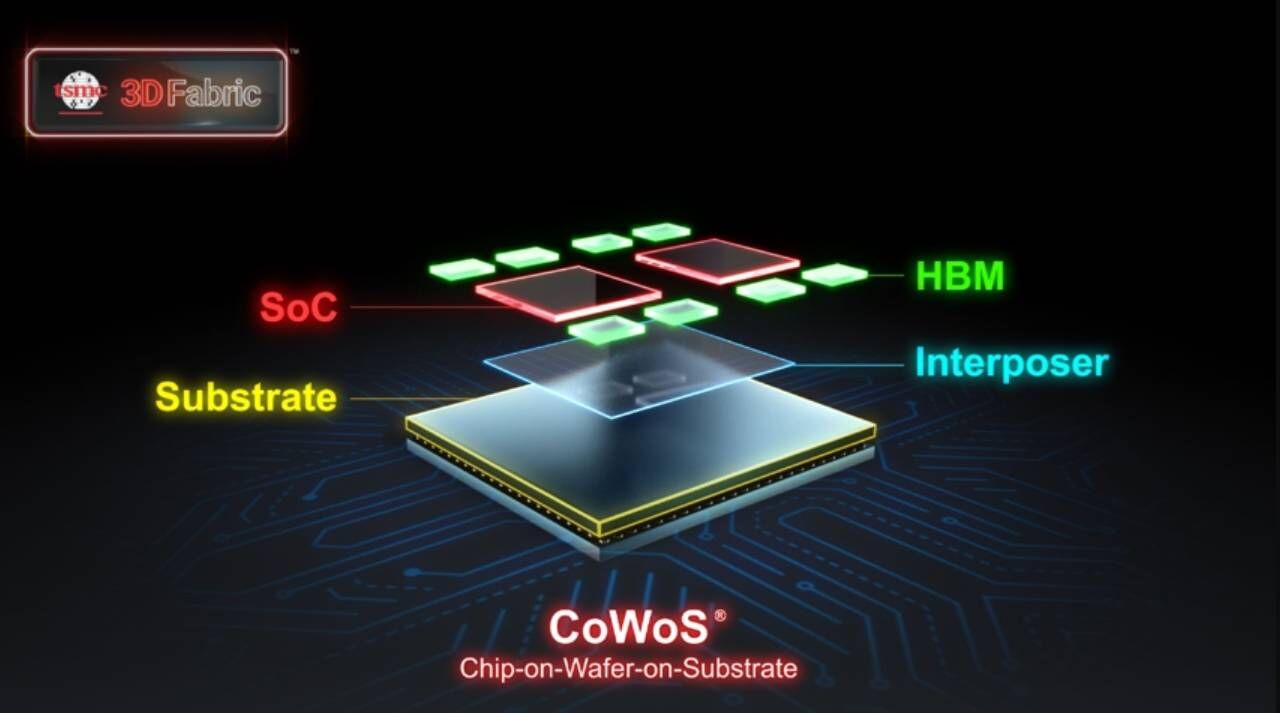
TSMC’s CoWoS capacity to reach 75,000 wafers/month by end-2025
onsemi expects to produce 200mm SiC wafers by 2025
Analyze the key factors and prospects of electronic components shortage from the perspective of wafer industry

Subscribe SemiMedia

Please check your E-mail to confirm the subscribtion.

Related posts

Vishay introduces automotive 1 MBd high speed optocoupler

Vishay introduces automotive 1 MBd high speed optocoupler

July 15, 2026
0
PSMC raises DRAM wafer prices by 40% to 45% amid tight AI-driven demand

PSMC raises DRAM wafer prices by 40% to 45% amid tight AI-driven demand

July 15, 2026
0
Tower Semiconductor to invest $3 billion in Japan chip manufacturing

Tower Semiconductor to invest $3 billion in Japan chip manufacturing

July 15, 2026
0
Bosch begins sample production at first U.S. silicon carbide chip fab

Bosch begins sample production at first U.S. silicon carbide chip fab

July 14, 2026
0
Copyright © 2017-2026 SemiMedia. Designed by nicetheme.
  • Breaking News
  • MarketWatch
  • Distribution
  • Manufacturer
  • Video
  • About us
  • electronic components news
  • Electronic components supplier
  • Electronic parts supplier
  • Electronic components distributor
  • Infineon
  • Electronic component news
  • Renesas
  • Vishay
  • STMicroelectronics
  • NXP

SemiMediaEdit

Administrator