

October 14, 2026 / SemiMedia / — Applied Materials has officially opened its Engineering and Process Innovation Center (EPIC) in Silicon Valley, bringing together TSMC, Intel, Samsung Electronics, Micron Technology and SK hynix as founding partners to accelerate next-generation semiconductor development.
Located at Applied Materials’ Sunnyvale, California campus, the EPIC Center represents a $5 billion investment and includes nearly four acres of advanced cleanroom space within a 600,000-square-foot facility. The center is designed to combine materials research, semiconductor equipment development and process optimization, helping shorten the transition from technology development to high-volume manufacturing.
Applied Materials CEO Gary Dickerson said AI infrastructure growth and high-performance computing are driving unprecedented semiconductor manufacturing complexity, requiring closer collaboration among chipmakers, equipment suppliers and research teams.
TSMC Chairman and CEO C.C. Wei said the company’s 30-year partnership with Applied Materials has supported technology transitions from 350nm processes to today’s 2nm generation. Through EPIC, the two companies will continue to collaborate on advanced process technologies, including new transistor structures, low-resistance interconnects and advanced packaging.
Intel CEO Lip-Bu Tan said AI is accelerating innovation in transistor technology, interconnects and advanced packaging, while future semiconductor systems will require deeper cooperation across the supply chain.
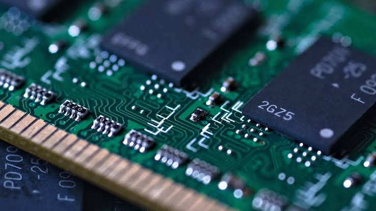
Memory manufacturers including Micron and SK hynix will use the platform to advance technologies related to HBM, DRAM and NAND, as AI workloads continue to increase demand for high-performance memory solutions.
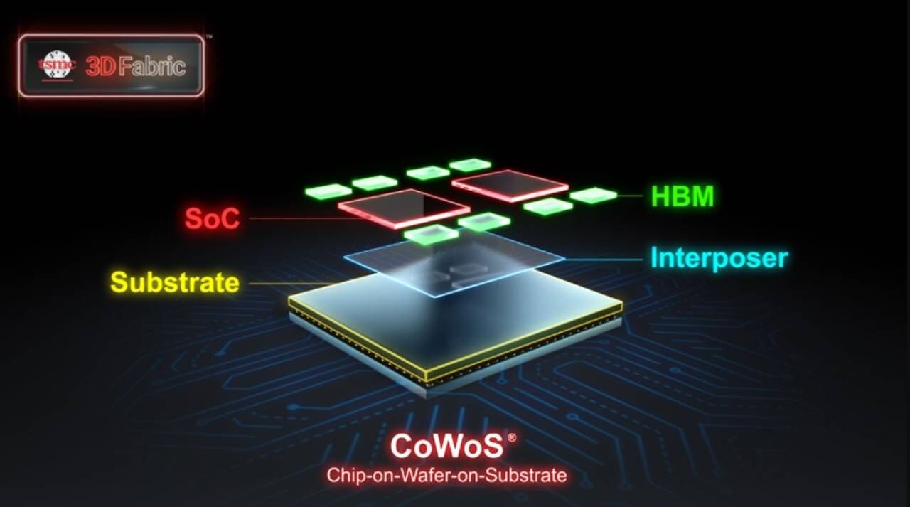
Advanced packaging is also a key focus area. As AI systems increasingly integrate logic chips, high-bandwidth memory and high-speed interconnects, companies are seeking new manufacturing approaches to improve performance and efficiency.
Applied Materials said EPIC will provide a collaborative environment where semiconductor companies can develop and optimize materials, equipment and processes earlier in the manufacturing cycle, helping accelerate the commercialization of future AI semiconductor technologies.




All Comments (0)