

Kioxia advances high-layer NAND to meet AI data center demand
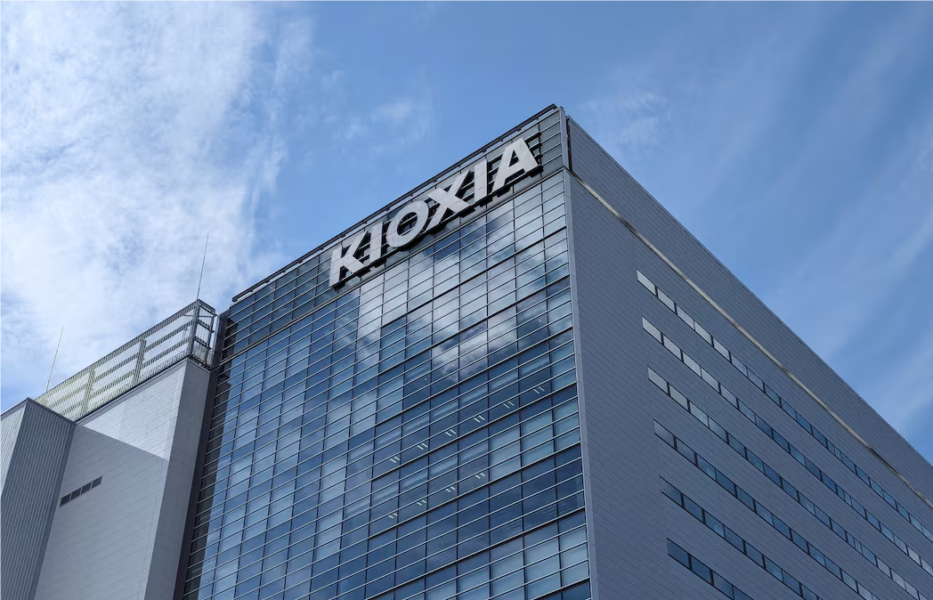
December 15, 2025 /SemiMedia/ — Japanese memory chipmaker Kioxia plans to start producing next-generation NAND flash in Iwate prefecture in 2026, as it steps up efforts to supply high-capacity storage for AI data centers.
The company’s Kitakami fab in northern Japan will handle mass production of its tenth-generation NAND technology. By increasing the number of vertically stacked memory layers to 332 from 218 in its eighth generation, Kioxia aims to boost storage density per chip area by about 59% while improving data transfer speeds by roughly 33% and lowering power consumption.
Industry sources said development work for the new NAND generation has largely taken place at Kioxia’s Yokkaichi plant in Mie prefecture, fuelling speculation that production would follow there. However, people familiar with the matter said volume manufacturing will instead be carried out in Kitakami, using the site’s second fabrication building, which began operations in September.
Dual-fab strategy separates high-performance and high-capacity NAND
The decision highlights Kioxia’s increasingly differentiated manufacturing strategy. The company is separating production roles between its major fabs, with Yokkaichi focused on high-performance and cost-sensitive products, while Kitakami is positioned for capital-intensive, high-layer-count NAND aimed at large-scale storage applications.
Kioxia plans to begin mass production of its ninth-generation NAND at the Yokkaichi plant by the end of the current fiscal year, primarily targeting smartphones and other consumer devices. That generation retains the same layer count as its predecessor but adopts an updated architecture to improve speed and energy efficiency.
The company has been using a direct wafer bonding approach since its eighth generation, producing memory cell wafers and logic circuit wafers separately before bonding them together, rather than integrating both on a single wafer. The design is intended to enhance performance while managing manufacturing complexity.
Iwate emerges as a new center for Japan’s memory chip manufacturing
Kioxia’s expansion is also contributing to the emergence of southern Iwate as a semiconductor manufacturing hub. Tokyo Electron recently opened a combined production and logistics facility in the area, while equipment suppliers such as Fujikin and Mirapro are increasing their local presence.




All Comments (0)