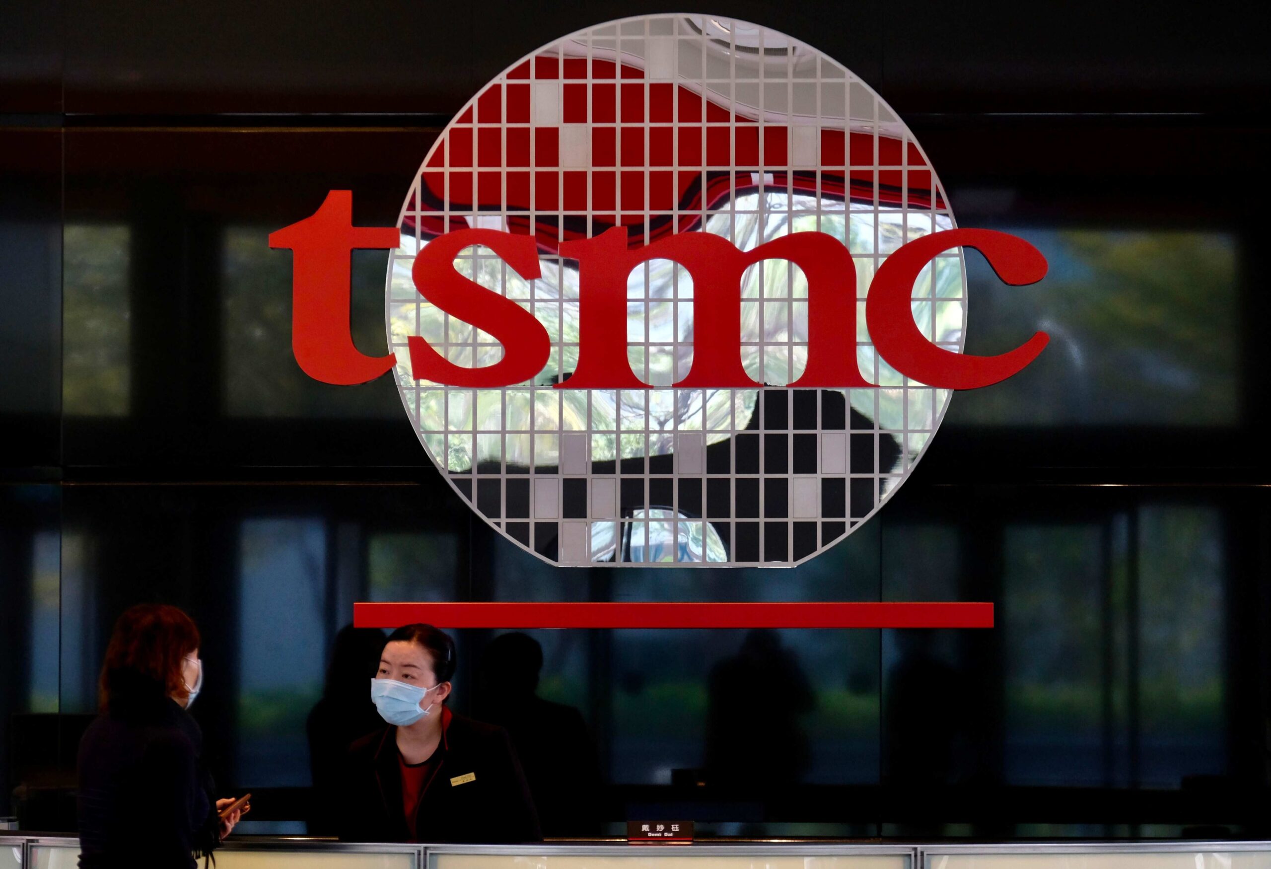
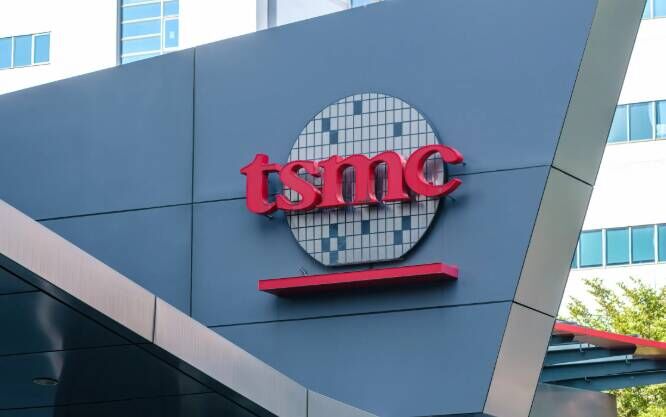
June 2, 2026 /SemiMedia/ — Nvidia said TSMC is adopting its accelerated computing and artificial intelligence technologies to improve semiconductor design, manufacturing and fab operations as advanced chip production becomes increasingly complex.
As process technologies move to more advanced nodes, turning chip designs into high-volume manufacturing has become one of the industry’s most demanding computing challenges. Computational lithography, transistor simulation, process control, wafer inspection and fab scheduling all require large-scale simulation, real-time optimization and advanced data analysis.
TSMC is using Nvidia GPUs, CUDA-X libraries and AI models across several parts of its semiconductor manufacturing workflow to shorten production cycles, improve energy efficiency, increase yield and optimize fab operations.
In computational lithography, TSMC is using Nvidia’s cuLitho GPU-accelerated library to improve mask design and lithography calculation efficiency. Compared with traditional CPU-based approaches, the technology can improve cost efficiency or cycle time by 20% to 50% at similar total cost of ownership, according to Nvidia.
For transistor, device and process simulation, TSMC is using Nvidia’s cuEST electronic structure simulation library for semiconductor materials design. GPU acceleration has increased chemical simulation speeds by an average of about 50 times.
In advanced process control, TSMC is using Nvidia’s cuML machine learning library to accelerate large-scale data analysis on GPUs. The system can process large numbers of production parameters across tens of thousands of manufacturing steps and feed them into machine learning models to reduce process variation.
Fab operations are another focus area. TSMC is using CUDA-based GPU acceleration for production scheduling, supported by Nvidia H200 GPUs. The approach is designed to help fabs manage complex manufacturing constraints, streamline production flows and improve capacity utilization.
For wafer inspection, TSMC is applying Nvidia Metropolis and the TAO toolkit to improve defect classification for advanced chips. Vision AI can help enhance nanoscale defect inspection while reducing the data-labeling and model-retraining workload when production environments, inspection equipment or defect types change.
TSMC is also exploring Nvidia Omniverse libraries to build a fab digital twin system known as FabTwin. The virtual fab environment can be used to evaluate equipment layouts and simulation workflows before physical deployment, helping identify bottlenecks and support faster planning decisions.
Nvidia Chief Executive Officer Jensen Huang said TSMC is applying AI and accelerated computing to fab operations to solve some of the world’s most difficult design and manufacturing challenges through simulation, optimization and artificial intelligence.
TSMC Chairman and Chief Executive Officer C.C. Wei said the use of Nvidia accelerated computing and AI in fab optimization, lithography, process control and inspection will strengthen the company’s technology leadership and manufacturing capabilities.


All Comments (0)