According to Herald Business Newspaper, Samsung Electronics has signed a contract with semiconductor equipment supplier ASML on January 15 to purchase about 20 EUV lithography equipment for US $ 3.38 billion, which is higher than Samsung ’s plan last October.
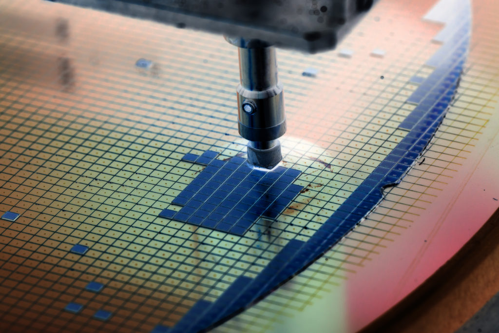
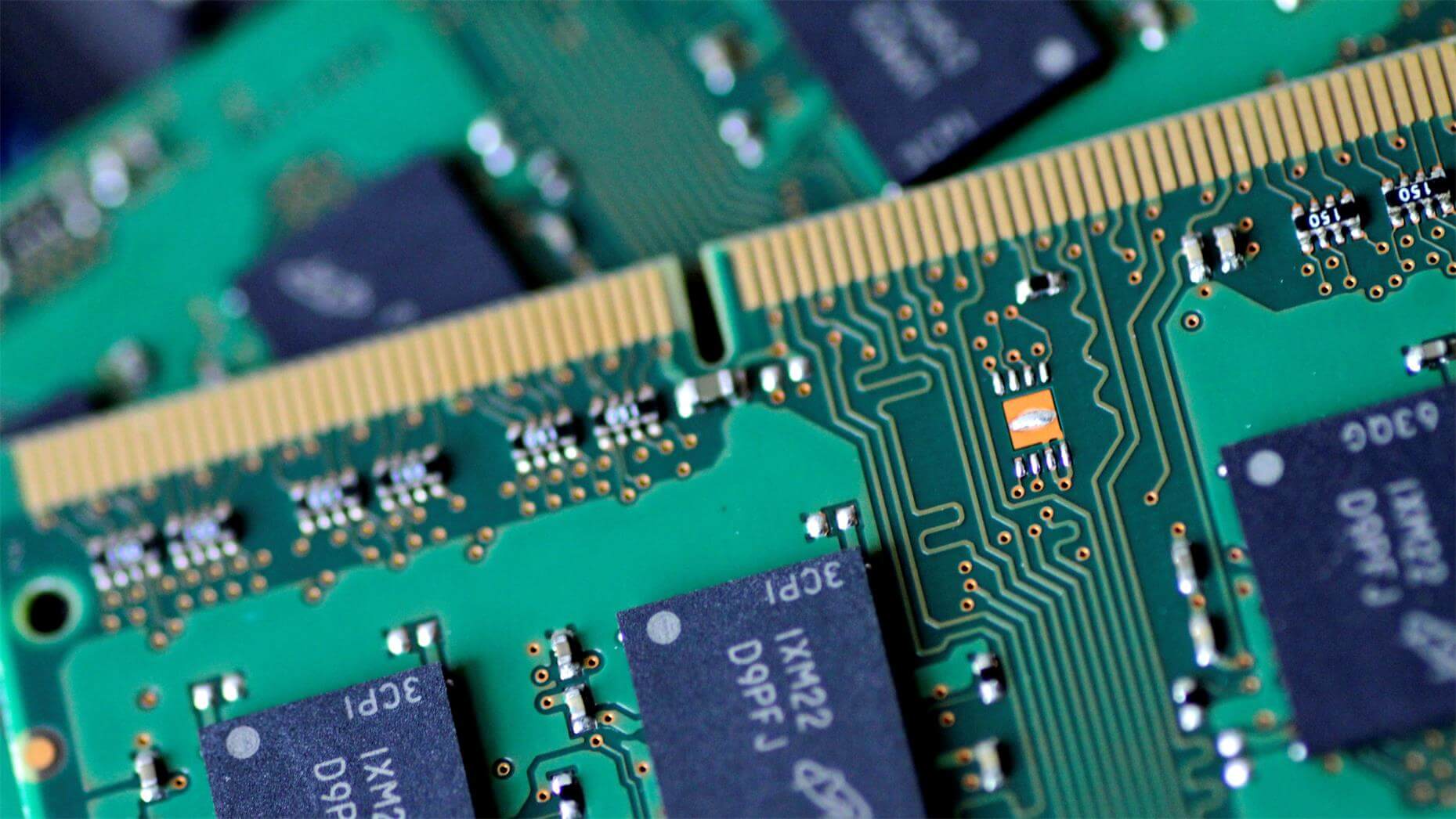
The report said that these EUV equipment will be delivered to Samsung within two years for the foundry business and the production of next-generation DRAM. It is reported that Samsung Electronics will first use EUV equipment to produce DRAM at the end of this year.
Samsung Electronics acquired a 3% stake in ASML in 2012 and contributed to the development of lithography machines. In order to surpass TSMC in the wafer foundry field, Samsung's key move is to attract customers by providing technological competitiveness on the basis of increasing investment.
Previously, Samsung Electronics planned to invest 133 trillion won to upgrade the semiconductor business by 2030. According to the plan, 73 trillion won of the 133 trillion won investment is technology research and development costs, and 60 trillion won is the construction of wafer fab infrastructure. Samsung's goal is to not only keep the lead in memory chips by 2030, but also to become a leader in logic chips.


All Comments (0)