September 4, 2025 /SemiMedia/ — Amkor Technology said it will build a $2 billion advanced packaging and testing facility in Peoria, Arizona, with production slated to begin in early 2028.
The facility, covering 104 acres, will be the most ambitious outsourced semiconductor packaging plant announced in the United States to date, underscoring efforts to bring backend manufacturing closer to U.S. wafer fabs. While TSMC and Intel push leading-edge wafer production domestically, packaging and final assembly have long been dominated by Taiwan and South Korea.
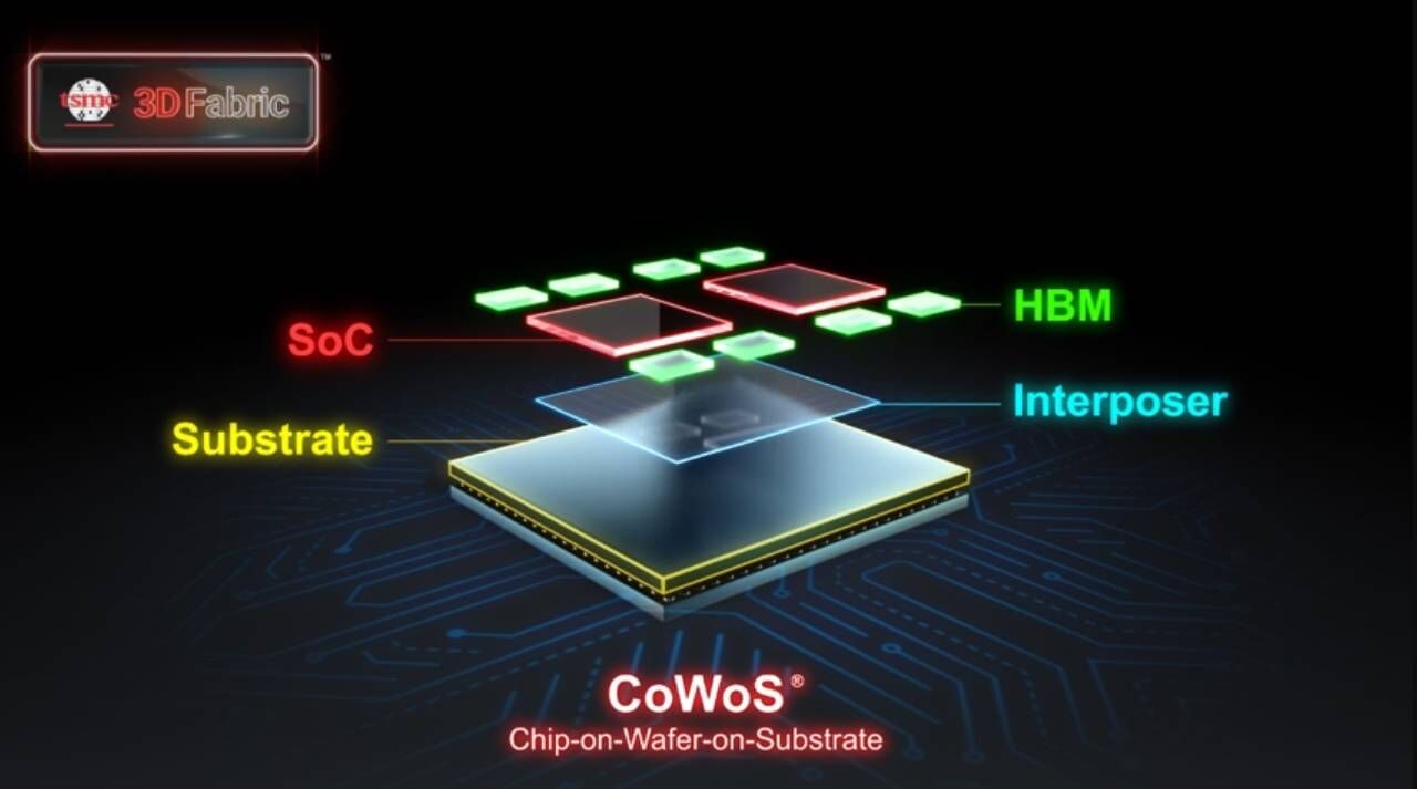
Amkor’s new site will focus on high-performance packaging platforms such as TSMC’s CoWoS and InFO, which underpin Nvidia’s data center GPUs and Apple’s latest processors. TSMC signed a memorandum of understanding to shift some packaging work from its Phoenix fab to the Amkor plant, reducing the weeks-long turnaround previously required to ship wafers back to Asia. Apple is expected to be among the first major customers.
The project will receive support from the U.S. CHIPS Act, including $407 million in funding and federal tax incentives. Amkor said the expansion aims to strengthen U.S. competitiveness in an industry increasingly defined by multi-chip complexity.
Still, the 2028 launch date means near-term supply bottlenecks for GPUs and AI servers will remain tied to Asia’s mature packaging lines. Beyond construction, Amkor faces a talent crunch, with U.S. chipmakers projected to face a workforce shortfall of 70,000 to 90,000 despite increased automation.







All Comments (0)