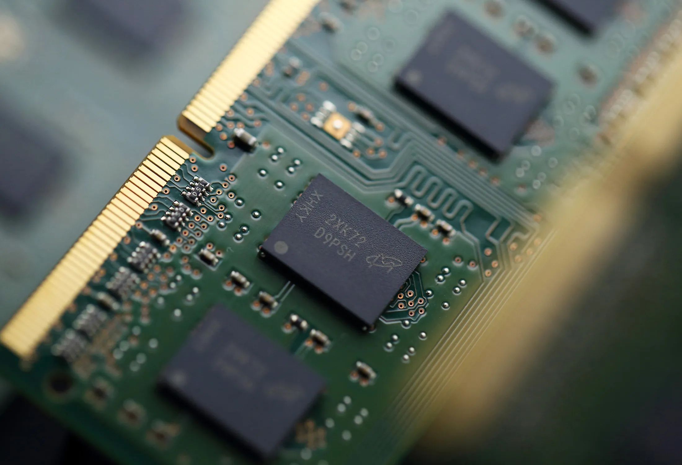
June 23, 2025 /SemiMedia/ — Samsung Electronics has significantly improved the production yield of its sixth-generation 10nm-class DRAM, with recent wafer tests showing yields of 50% to 70%, according to industry sources. This marks a substantial leap from sub-30% yields recorded in the same process last year.
The company reportedly implemented a series of design optimizations to enhance performance and efficiency, opting to delay mass production to refine its architecture. Samsung had initially targeted year-end 2023 for mass production but chose to rework the chip structure, accepting a timeline shift in exchange for long-term gains. Production lines were prepared in advance to allow rapid deployment once final tests were complete.
The improved process is expected to strengthen Samsung’s competitiveness in HBM4 production. DRAM chips for mobile (LPDDR) and server applications will be manufactured at its Pyeongtaek Line 4, while HBM4-oriented production leveraging the same 10nm-class DRAM process will be based at Pyeongtaek Line 3.
Industry experts note that the core storage cell architecture is largely shared between DRAM for standard applications and HBM, meaning improvements in one can directly enhance the yield and scalability of the other. Based on these advances, Samsung is reportedly considering expanded investment in HBM4 infrastructure at Pyeongtaek.
While it remains to be seen whether Samsung will revisit its strategy of leveraging economies of scale to gain market share, the company retains a clear advantage in both tangible and intangible resources across development and production.


All Comments (0)