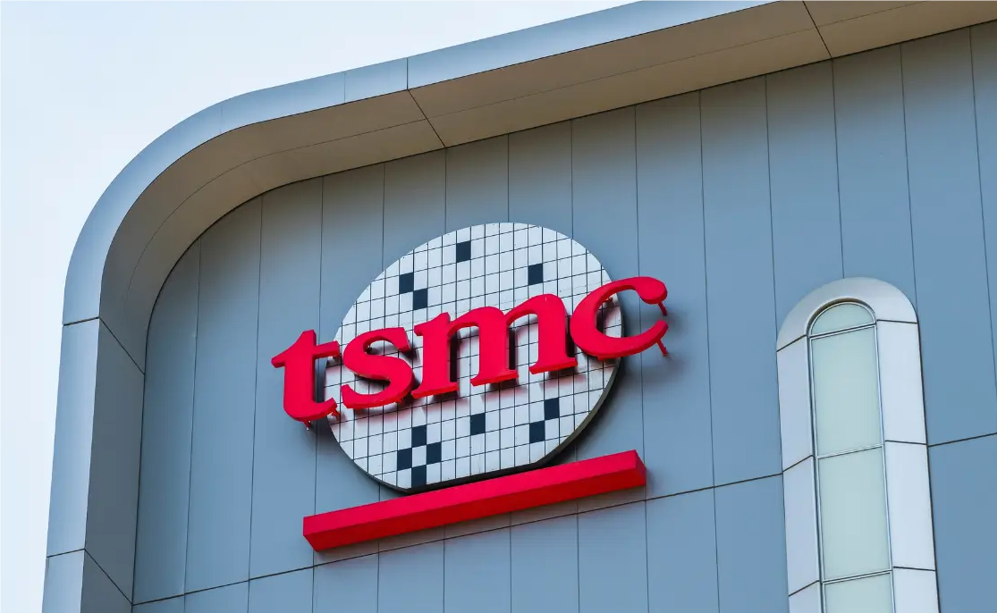
June 6, 2025 /SemiMedia/ — Taiwan Semiconductor Manufacturing Co. (TSMC) is reportedly pricing its forthcoming 1.6nm (A14) process at up to $45,000 per wafer, marking a 50% increase over its 3nm pricing and reflecting the growing cost of leading-edge semiconductor production.
Wafer pricing in foundry services is driven by factors such as R&D investment, production scale, and customer-specific agreements. Long-term partner Apple is believed to secure more favorable rates, while companies like AMD, NVIDIA, Intel, and Qualcomm are more dependent on their order volumes.
Historically, wafer costs have surged with each process shrink—from around $2,000 per wafer at 90nm in 2004 to $10,000 at 7nm, $16,000 at 5nm, and nearly $20,000 for 3nm.
TSMC’s 2nm (N2) node, scheduled for mass production later this year, is expected to be adopted by Apple’s A20 and M6 chips and AMD’s Zen 6 EPYC processors. The upcoming A16 node, planned for 2026, integrates nanosheet transistors, backside power delivery, and super rails, offering a 8–10% performance boost, 15–20% power reduction, and 10% higher transistor density compared to N2P.
Looking further ahead, the A14 node will introduce second-generation GAAFET transistors and a new NanoFlex Pro standard cell architecture. It is expected to deliver 10–15% higher performance, 25–30% lower power consumption, and a 23% increase in density over N2. Volume production is slated for early 2028, and costs are projected to rise accordingly.
Adding to the complexity, the success rate of first-time tape-outs has dropped to just 14%, down 10 percentage points from two years ago, exacerbating development risks and costs for chipmakers.


All Comments (0)