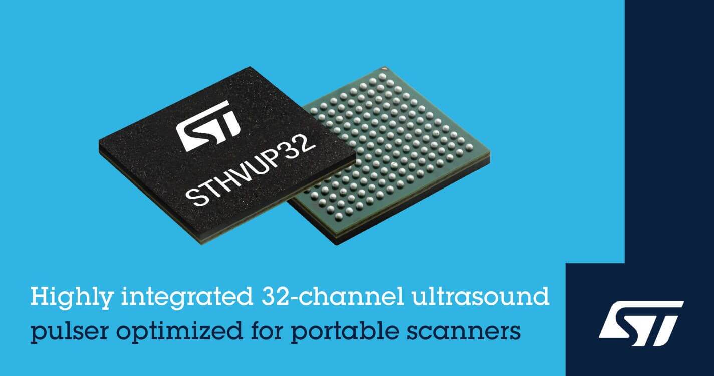
Feb. 16, 2023 /SemiMedia/ -- STMicroelectronics announces the expansion of its range of advanced ultrasonic transmitters by offering a new ±800mA transmitter, the STHVUP32, for portable systems requiring extra drive capability for a coaxial cable-mounted probe.
Joining the portfolio alongside the 64-channel STHVUP64, the new 32-channel version contains similar features to increase performance and integration in next-generation affordable, high-performing scanners for medical and industrial applications. These include innovations to maximize image quality, built-in digital beam steering, a space-saving driver architecture, and low power consumption.
The STHVUP32 has 5-level output capability, in addition to the common 3-level output, which enhances flexibility to optimize the picture quality. Its high output current allows driving the scanner’s piezoelectric transducer at high speed to enable multiple imaging modes. It also helps achieve minimum pulse duration of 5ns for superior image detail. The transmitter supports continuous-wave (CW) and pulsed-wave (PW) operating modes to allow various types of analysis including cavities and liquid flow.
The digital beam steering enhances directional control by permitting greater precision than conventional analog steering using delay circuits. By integrating the beam-steering logic, the transmitter can be used without a companion chip such as an FPGA. This saves PCB space and routing complexity, as well as bypassing FPGA-design challenges.
Also new, the transmitter has a self-biased driver architecture that saves connecting decoupling capacitors to the transmitter’s power-supply pins. This helps ensure a smaller circuit footprint, as well as lowering the bill of materials (BOM). In addition, the STHVUP32 is housed in a smaller package than comparable alternative ICs thereby helping designers create next-generation products in even smaller form factors.
While having extremely low power consumption, which is key for battery-operated systems, the STHVUP32 is richly featured for a superior user experience. There is on-chip memory for storing transmission patterns, and synchronization is possible using a clock signal up to 200MHz to enhance image quality by minimizing jitter. The IC also provides a communication port that supports multiple CMOS signaling standards.
Built-in protection includes noise blocking, thermal protection, under-voltage protection, and recirculating current protection. There is also a diagnostic register that allows directly reading the causes of interrupts to ease debugging in the event of a malfunction.
The STHVUP32 is built using ST’s proven BCD8s-SOI technology that supports analog (bipolar), digital (CMOS), and power (DMOS) circuits on the same die. It’s in production now, in a 11.5mm x 10.5mm x 1.35mm 168-ball FC-BGA168 package, and available at $84.00 each for orders of 1000 units.
For more information, please visit https://www.st.com/en/switches-and-multiplexers/sthvup32.html?icmp=tt30854_gl_pron_feb2023.


All Comments (0)