SemiMedia SemiMedia
  • Breaking News
  • MarketWatch
  • Distribution
  • Manufacturer
  • Video
  • About us
Home › MarketWatch › Samsung announces mass production of 14nm EUV DDR5 DRAM
  • 0

Samsung announces mass production of 14nm EUV DDR5 DRAM

SemiMediaEdit
October 12, 2021

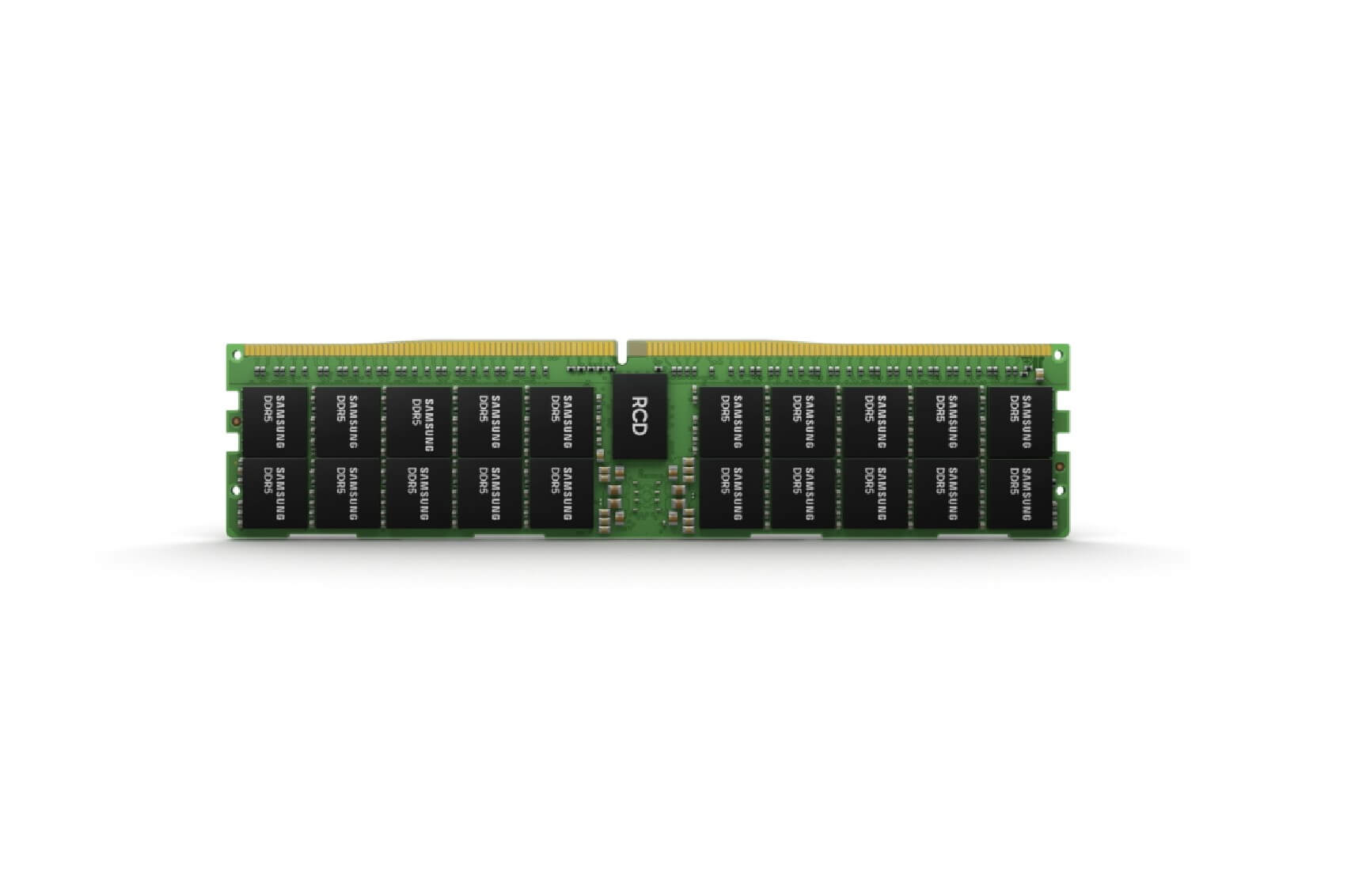
Samsung Electronics today announced that it has begun mass producing the industry's smallest, 14-nanometer (nm), DRAM based on extreme ultraviolet (EUV) technology. Following the company’s shipment of the industry-first EUV DRAM in March of last year, Samsung has increased the number of EUV layers to five to deliver today’s finest, most advanced DRAM process for its DDR5 solutions.

“We have led the DRAM market for nearly three decades by pioneering key patterning technology innovations,” said Jooyoung Lee, senior vice president and head of DRAM Product & Technology at Samsung Electronics. “Today, Samsung is setting another technology milestone with multi-layer EUV that has enabled extreme miniaturization at 14nm — a feat not possible with the conventional argon fluoride (ArF) process. Building on this advancement, we will continue to provide the most differentiated memory solutions by fully addressing the need for greater performance and capacity in the data-driven world of 5G, AI and the metaverse.”

As DRAM continues to scale down the 10nm-range, EUV technology becomes increasingly important to improve patterning accuracy for higher performance and greater yields. By applying five EUV layers to its 14nm DRAM, Samsung has achieved the highest bit density while enhancing the overall wafer productivity by approximately 20%. Additionally, the 14nm process can help bring down power consumption by nearly 20% compared to the previous-generation DRAM node.

Leveraging the latest DDR5 standard, Samsung’s 14nm DRAM will help unlock unprecedented speeds of up to 7.2 gigabits per second (Gbps), which is more than twice the DDR4 speed of up to 3.2Gbps.

Samsung plans to expand its 14nm DDR5 portfolio to support data center, supercomputer and enterprise server applications. Also, Samsung expects to grow its 14nm DRAM chip density to 24Gb in better meeting the rapidly-growing data demands of global IT systems.

Related

DDR5 electronic components news SAMSUNG
Nexperia announces surface mount device have passed board-level reliability requirements for automotive applications
Previous
ADI ends relationship between Maxim and Avnet and signs Arrow as global distributor
Next

All Comments (0)

Back
No Comment.

Top Post

Fire broke out at AKM factory in Japan
Qualcomm ranked first in the world's top ten IC design companies
Mouser Electronics expands to the Philippines with local customer service center
Analyze the key factors and prospects of electronic components shortage from the perspective of wafer industry
What is the root cause of the decline of the Japanese semiconductor industry?
ST releases price increase notice

Subscribe SemiMedia

Please check your E-mail to confirm the subscribtion.

Related posts

Intel weighs sale of networking and edge unit to sharpen chip focus

Intel weighs sale of networking and edge unit to sharpen chip focus

May 22, 2025
0
Wolfspeed bankruptcy may shift SiC orders to Taiwan-based suppliers

Wolfspeed bankruptcy may shift SiC orders to Taiwan-based suppliers

May 22, 2025
0
onsemi unveils SiC-based IPM to boost power efficiency in industrial and AI data center systems

onsemi unveils SiC-based IPM to boost power efficiency in industrial and AI data center systems

May 21, 2025
0
Wolfspeed nears bankruptcy as SiC chipmaker struggles with debt

Wolfspeed nears bankruptcy as SiC chipmaker struggles with debt

May 21, 2025
0
Copyright © 2017-2025 SemiMedia. Designed by nicetheme.
  • Please set up your first menu at [Admin -> Appearance -> Menus]
  • electronic components news
  • Electronic components supplier
  • Electronic parts supplier
  • Infineon
  • Electronic component news
  • Renesas
  • Vishay
  • STMicroelectronics
  • NXP
  • TDK

SemiMediaEdit

Administrator