
SemiMedia SemiMedia
  • Breaking News
  • MarketWatch
  • Distribution
  • Manufacturer
  • Video
  • About us
Home › MarketWatch › SK Hynix invests over 120 trillion won to build 4 wafer fabs
  • 0

SK Hynix invests over 120 trillion won to build 4 wafer fabs

SemiMediaEdit
March 26, 2024

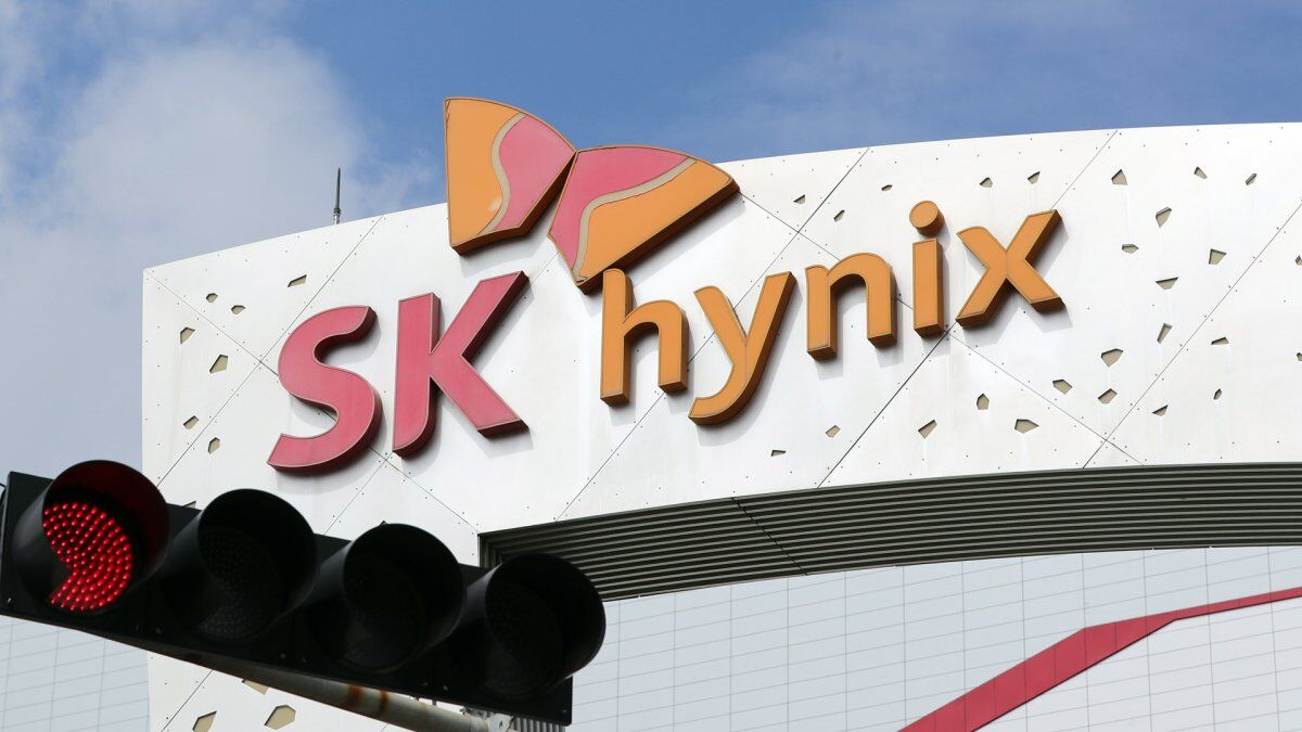
March 26, 2024 /SemiMedia/ -- According to reports, SK Hynix will start building semiconductor fabs in the Yongin Semiconductor Cluster in Gyeonggi-do, South Korea in March 2025. Starting from this, more than 120 trillion won (approximately US$89.245 billion) will be invested by 2046 to build a total of 4 wafer fabs.

SK Hynix had announced the plan as early as 2019, but it has been delayed due to licensing issues. SK hynix said the plan has made progress through an agreement reached by central and local governments and companies in 2022.

SK Hynix said that the first wafer fab is scheduled to start construction in March next year and will be the world's largest three-story wafer fab.

In addition, the Korean government will announce a strategy to accelerate AI chip exports and strengthen semiconductor facilities before the end of June. It will make every effort to ensure that Korean companies do not fall behind in the global semiconductor manufacturing field and actively support high-bandwidth memory (HBM) chip manufacturing.
Related

electronic components news Electronic components supplier Electronic parts supplier Semiconductor cluster SK Hynix
Samsung expects chip revenue to return to 2022 levels this year
Previous
Infineon launches industry’s first wide input voltage hot-swappable controller for telecom infrastructure
Next

All Comments (0)

Back
No Comment.

Top Post

Mouser Electronics expands to the Philippines with local customer service center
Fire broke out at AKM factory in Japan
Qualcomm ranked first in the world's top ten IC design companies
TSMC’s CoWoS capacity to reach 75,000 wafers/month by end-2025
onsemi expects to produce 200mm SiC wafers by 2025
Analyze the key factors and prospects of electronic components shortage from the perspective of wafer industry

Subscribe SemiMedia

Please check your E-mail to confirm the subscribtion.

Related posts

ASE unveils 310 mm panel-level packaging line for next-generation AI and HPC chips

ASE unveils 310 mm panel-level packaging line for next-generation AI and HPC chips

May 29, 2026
0
ST issues new price increase notice effective June 28

ST issues new price increase notice effective June 28

May 29, 2026
0
PKC expands high-purity chlorine capacity by 50% to support Samsung’s advanced chip production

PKC expands high-purity chlorine capacity by 50% to support Samsung’s advanced chip production

May 29, 2026
0
Samsung to invest $1.5 billion in Vietnam for first chip testing facility

Samsung to invest $1.5 billion in Vietnam for first chip testing facility

May 28, 2026
0
Copyright © 2017-2026 SemiMedia. Designed by nicetheme.
  • Breaking News
  • MarketWatch
  • Distribution
  • Manufacturer
  • Video
  • About us
  • electronic components news
  • Electronic components supplier
  • Electronic parts supplier
  • Infineon
  • Electronic component news
  • Electronic components distributor
  • Renesas
  • Vishay
  • STMicroelectronics
  • NXP

SemiMediaEdit

Administrator