
SemiMedia SemiMedia
  • Breaking News
  • MarketWatch
  • Distribution
  • Manufacturer
  • Video
  • About us
Home › MarketWatch › Samsung plans to break ground on its P3 fab in Pyeongtaek in September
  • 0

Samsung plans to break ground on its P3 fab in Pyeongtaek in September

SemiMediaEdit
August 11, 2020

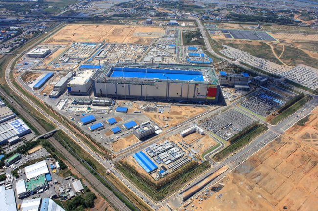
According to local South Korean media reports, industry insiders said yesterday that Samsung Electronics will start construction of its wafer fab in Pyeongtaek, South Korea as early as September.

According to Pyeongtaek government officials, Samsung had already carried out preparatory work in Pyeongtaek City in June. Recently, Samsung requested local government departments to issue construction permits as soon as possible, which shows that the company hopes to start the construction of the fab as soon as possible.

The total investment in the construction of P3 is estimated to be approximately US$25.2 billion, and it will become Samsung's largest fab in Pyeongtaek. In addition, Samsung plans to build three more wafer fabs in Pyeongtaek City in the future.

Currently, Samsung's P1 wafer fab is in operation, and P2 is also preparing to start full operation next year. Industry insiders speculate that P3 may start mass production in the second half of 2023.

In addition to P1, P2, and P3, Pyeongtaek officials said that Samsung is speeding up its plans for the other three fabs, the P4, P5, and P6.

Related

electronic components news Samsung P1 fab Samsung P2 fab Samsung P3 fab Samsung P4 fab Samsung P5 fab Samsung P6 fab Samsung Pyeongtaek
JSCJ's new IC packaging and testing plant in Suqian, Jiangsu will be put into use this month
Previous
KEMET announces new tantalum polymer capacitors for applications requiring high capacitance and high voltage
Next

All Comments (0)

Back
No Comment.

Top Post

Mouser Electronics expands to the Philippines with local customer service center
Fire broke out at AKM factory in Japan
Qualcomm ranked first in the world's top ten IC design companies
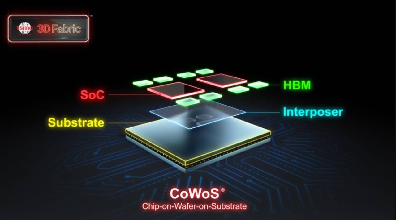
TSMC’s CoWoS capacity to reach 75,000 wafers/month by end-2025
onsemi expects to produce 200mm SiC wafers by 2025
Analyze the key factors and prospects of electronic components shortage from the perspective of wafer industry

Subscribe SemiMedia

Please check your E-mail to confirm the subscribtion.

Related posts

ASE unveils 310 mm panel-level packaging line for next-generation AI and HPC chips

ASE unveils 310 mm panel-level packaging line for next-generation AI and HPC chips

May 29, 2026
0
ST issues new price increase notice effective June 28

ST issues new price increase notice effective June 28

May 29, 2026
0
PKC expands high-purity chlorine capacity by 50% to support Samsung’s advanced chip production

PKC expands high-purity chlorine capacity by 50% to support Samsung’s advanced chip production

May 29, 2026
0
Samsung to invest $1.5 billion in Vietnam for first chip testing facility

Samsung to invest $1.5 billion in Vietnam for first chip testing facility

May 28, 2026
0
Copyright © 2017-2026 SemiMedia. Designed by nicetheme.
  • Breaking News
  • MarketWatch
  • Distribution
  • Manufacturer
  • Video
  • About us
  • electronic components news
  • Electronic components supplier
  • Electronic parts supplier
  • Infineon
  • Electronic component news
  • Electronic components distributor
  • Renesas
  • Vishay
  • STMicroelectronics
  • NXP

SemiMediaEdit

Administrator