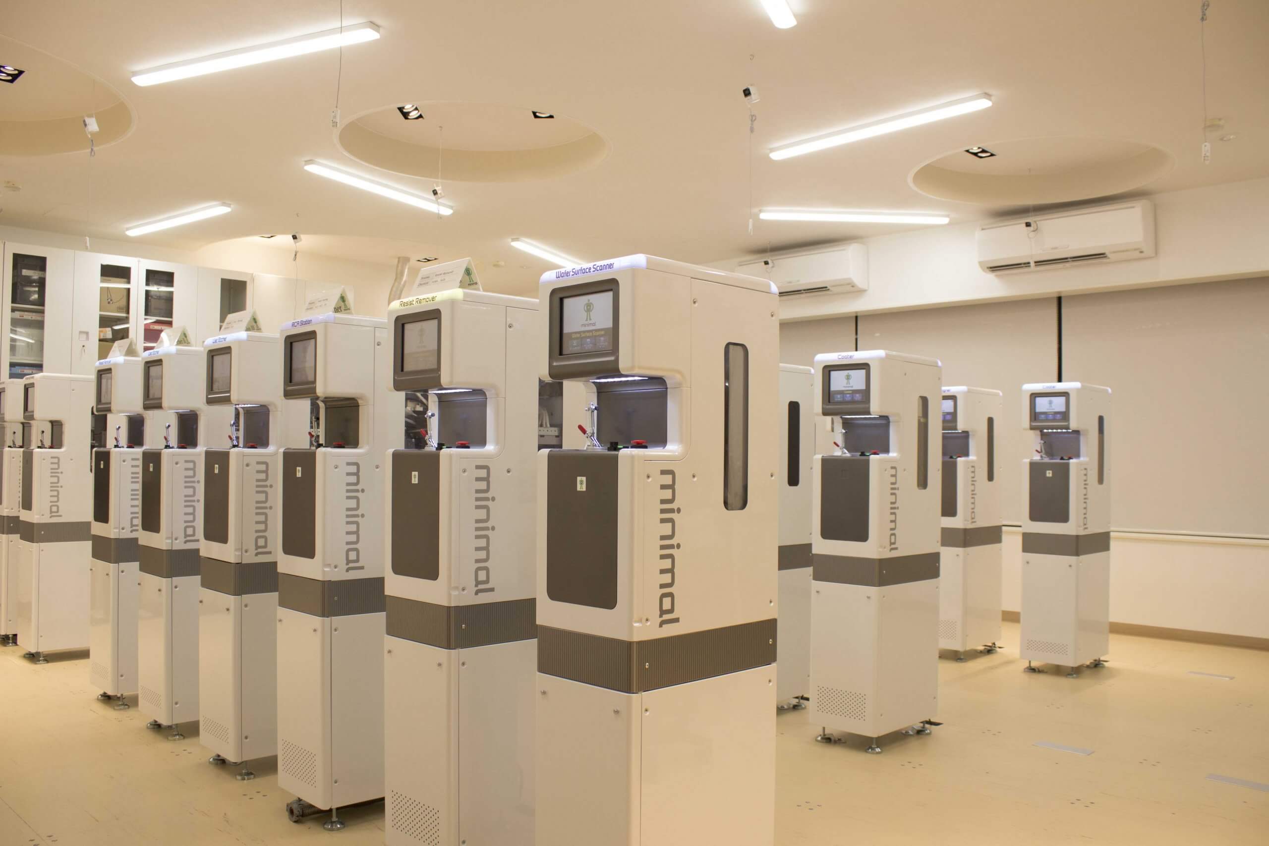
According to reports, Yokogawa brought AIST, Japan-originated Minimal Fab project to production. It uses 0.5-inch wafers and does not need a clean room to operate:
At present, the world’s largest wafer fab is TSMC’s GIGAFAB, which can produce more than 100,000 12-inch wafers per month, with a construction cost of up to 10 billion US dollars per fab. However, this Minimal Fab, which is aimed at sensor demand in the Internet of Things, starts at only $5.8 million.
This new-generation manufacturing system, led by the Ministry of Economy, Trade and Industry of Japan and jointly developed by 140 Japanese companies and organizations, aims to enable automobile and home appliance manufacturers to produce the required semiconductors and sensors through a significant reduction in cost and technology thresholds.
This production system is sold by Yokogawa Solutions, a subsidiary of Japan's Yokogawa Electric Group. These manufacturing machines are about the same size as beverage vending machines, but each has functions such as washing, heating, and exposure. Each machine is equivalent to a production line for semiconductor manufacturing. The minimum area required for a mini-fab production line is about the size of two tennis courts, which is only one-hundredth of the area of a 12-inch fab.
The mini-fab can be so cheap and small, first of all because it does not need a clean room.
If there is dust over 0.1 micron on the semiconductor chip, it is considered defective. For this reason, the manufacturing room must maintain an ultra-high cleanliness. In response to this challenge, the mini fab has a key technology for partial dust-free, Minimal Shuttle, which uses electromagnets to control the switch, and there is almost no dust entering.
Another advantage of the mini-fab is that it does not need to use photomask, which in turn can significantly reduce costs.
The annual output of mini fabs is about 500,000, while12-inch fab are 200 million. If only 10,000 pieces are produced, each chip on the market will charge $95, but the mini-fab will only charge $12.
The research and development plan of the mini fab started in 2010. A total of 140 corporate groups participated, including many major manufacturers. Although it is sold by Yokogawa Solutions, there are about 30 Japanese SMEs participating in the development and manufacturing, which is also one of the major features of the equipment.
According to the original plan, the equipment required for the semiconductor front-end process of the mini-fab has been roughly completed in 2016. And before 2018, the subsequent process equipment such as chip cutting function and packaging will also be developed. Yokogawa's announcement of putting its mini fab into production is an important step for the industry.


All Comments (0)