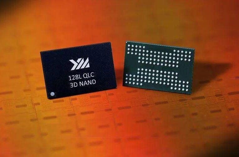
Chinese memory chip manufacturer Yangtze Memory Technologies Co., Ltd (YMTC) announced yesterday that its 128-layer 1.33Tb QLC 3D NAND flash memory chip, X2-6070, has passed sample verification on the SSD platform through co-working with multiple controller partners. As the first QLC based 128-layer 3D NAND, X2-6070 has achieved the highest bit density, highest I/O speed and highest capacity so far among all released flash memory parts in the industry①. Accompanying this release, YMTC introduced a 128-layer 512Gb TLC (3 bit/cell) chip, X2-9060, to meet diversified application requirements.
“As a new entrant in the flash memory industry, YMTC has reached to new heights by launching the 1.33 Tb QLC product,’’ said Grace Gong, YMTC Senior Vice President of Marketing and Sales. “We are able to achieve these results today because of the incredible synergy created through seamless collaboration with our global industry partners, as well as remarkable contributions from our employees. With the launch of XtackingTM 2.0, YMTC is now capable of building a new business ecosystem where our partners can play to their strengths and we can achieve mutually beneficial results.”
Leveraging the innovative XtackingTM architecture, YMTC has optimized the design and manufacturing processes of CMOS circuits and memory arrays. As a result, YMTC’s 64-layer TLC products perform well in terms of storage bit density, I/O speed, and reliability.
In its 128-layer line of products, XtackingTM has been upgraded to version 2.0, which is bringing more benefits to flash memory. In terms of read/write performance, 1.6Gbps can be enabled on both X2-6070 and X2-9060 by using 1.2V Vccq, which is so far the highest I/O speed in the industry. As independent manufacturing processes have been adopted for peripheral circuits and memory cells, it provides the capability to bring better functional scalability in chip design without increasing the chip area. In the future, YMTC will continue to collaborate with more partners to build its ecosystem and benefit the industry through technology innovation.
Compared with TLC, QLC has notable features including large capacity, cost-effectiveness, and efficiency for read-intensive applications. Each X2-6070 QLC chip has 128 layers of array stacks and contains more than 366 billion effective charge-trap memory cells. As a single memory cell contains 4-bit data, each chip provides a total of 1.33 Tb storage capacity.
YMTC said that the chip is expected to be mass-produced from the end of 2020 to the middle of 2021, with a target of 100,000 pieces per month.


All Comments (0)