July 11, 2025 /SemiMedia/ — Taiwan Semiconductor Manufacturing Co. (TSMC) is accelerating its advanced packaging investments in the United States, with two new facilities expected to begin construction in 2028. The planned sites will focus on SoIC and CoPoS technologies to support growing demand for local AI and HPC chip packaging.
According to industry sources, these packaging plants will be located adjacent to TSMC’s third Arizona wafer fab (F21 P3), which will adopt N2 (2nm) and A16 process technologies. Equipment move-in for the fab is scheduled for Q2 2025. TSMC has also indicated that a fourth fab will use the same nodes, while future fabs may adopt even more advanced technologies depending on customer requirements.
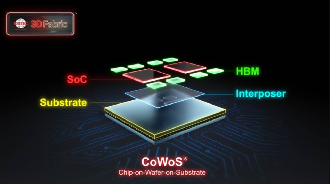
Unlike the widely used CoWoS, the US sites will initially implement SoIC and CoPoS packaging. SoIC is currently TSMC’s most mature 3D integration technology in production and is expected to be integrated with CoWoS and future CoPoS flows. AMD has already adopted SoIC in high-volume production, and other major clients such as Apple, NVIDIA, and Broadcom are also exploring its use in high-end products.
CoPoS remains in its early stages, with a pilot line planned for 2026. Mass production, however, will be centered at the AP7 site in Chiayi, Taiwan, starting between late 2028 and 2029.
The expansion reinforces TSMC’s strategic role in the US semiconductor ecosystem and strengthens its ability to deliver advanced chip packaging solutions locally for next-generation AI and HPC applications.






All Comments (0)