SemiMedia SemiMedia
  • Breaking News
  • MarketWatch
  • Distribution
  • Manufacturer
  • Video
  • About us
Home › MarketWatch › TSMC begins construction of third fab in Arizona to expand U.S. chip capacity
  • 0

TSMC begins construction of third fab in Arizona to expand U.S. chip capacity

SemiMediaEdit
May 1, 2025

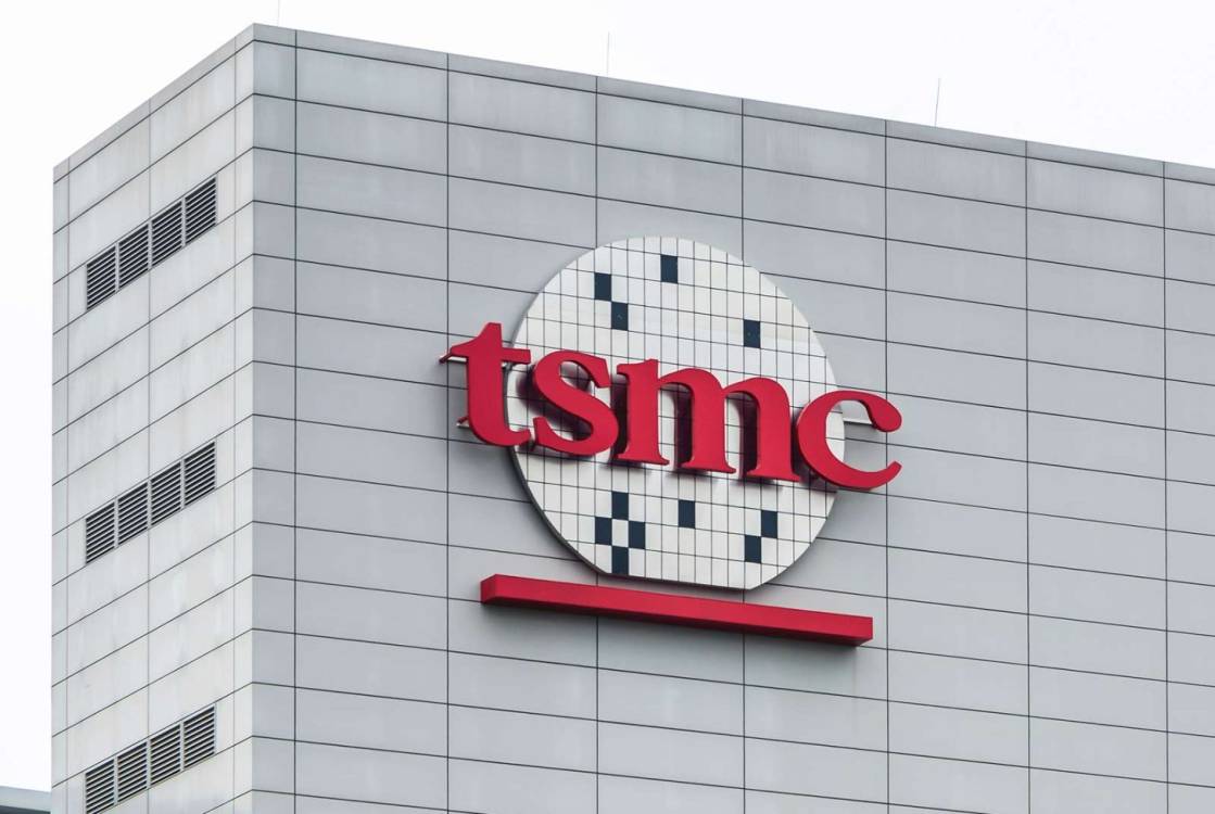
May 1, 2025 /SemiMedia/ — TSMC has broken ground on its third wafer fabrication facility in Arizona, accelerating its U.S. expansion plans as the company responds to rising demand for domestic chip production and competitive foundry dynamics.

The announcement coincided with a site visit from U.S. Commerce Secretary Howard Lutnick and marks the launch of TSMC’s third phase in the U.S., which the company described as the largest single foreign direct investment in American history.

TSMC, a key supplier to Apple and NVIDIA, is central to U.S. efforts to localize semiconductor production. In March, CEO C.C. Wei joined former President Donald Trump at the White House to unveil an additional $100 billion investment aimed at boosting U.S. chip output. This brings TSMC’s total planned U.S. investment to $165 billion.

Under its current roadmap, TSMC aims to establish six advanced wafer fabs and two advanced packaging facilities in the U.S., supporting next-generation technologies across AI, HPC, and automotive sectors.

Related

advanced chip production CHIPS Act funding electronic components news Electronic components supplier Electronic parts supplier foundry investment semiconductor manufacturing USA TSMC Arizona fab U.S. chip expansion
Global silicon wafer shipments rise 2.2% year-on-year but fall on quarter
Previous
EU chip strategy under pressure as 2030 market share goal deemed unrealistic
Next

All Comments (0)

Back
No Comment.

Top Post

Fire broke out at AKM factory in Japan
Mouser Electronics expands to the Philippines with local customer service center
Qualcomm ranked first in the world's top ten IC design companies
Analyze the key factors and prospects of electronic components shortage from the perspective of wafer industry
What is the root cause of the decline of the Japanese semiconductor industry?
onsemi expects to produce 200mm SiC wafers by 2025

Subscribe SemiMedia

Please check your E-mail to confirm the subscribtion.

Related posts

Kioxia plans 332-layer NAND output in Iwate to target AI data center demand

Kioxia plans 332-layer NAND output in Iwate to target AI data center demand

December 15, 2025
0
TE to raise connector prices from early 2026, impacting chip supply chain

TE to raise connector prices from early 2026, impacting chip supply chain

December 15, 2025
0
Japan’s top banks signal up to $13 billion financing for Rapidus 2nm chip push

Japan’s top banks signal up to $13 billion financing for Rapidus 2nm chip push

December 15, 2025
0
South Korea weighs $3 billion plan to build new foundry to boost chip ecosystem

South Korea weighs $3 billion plan to build new foundry to boost chip ecosystem

December 12, 2025
0
Copyright © 2017-2025 SemiMedia. Designed by nicetheme.
  • Please set up your first menu at [Admin -> Appearance -> Menus]
  • electronic components news
  • Electronic components supplier
  • Electronic parts supplier
  • Infineon
  • Electronic component news
  • Renesas
  • Vishay
  • STMicroelectronics
  • NXP
  • TDK

SemiMediaEdit

Administrator