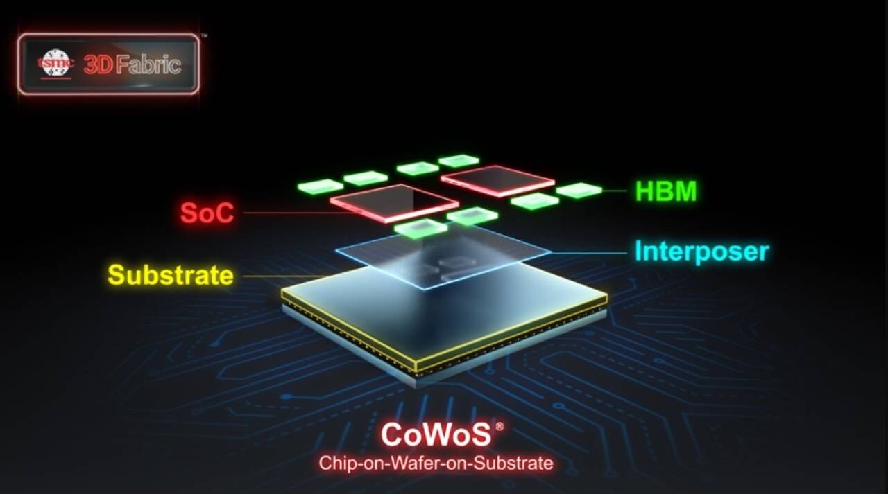
March 11, 2024 /SemiMedia/ -- According to reports, SK Hynix is increasing its spending on advanced chip packaging in order to better meet the growing demand for HBM (high-bandwidth memory), a key component in the development of artificial intelligence (AI).
Lee Kang-Wook, SK Hynix's vice president in charge of packaging development, said the company is investing more than $1 billion in South Korea to expand and improve its chip packaging. The innovation of this packaging process will further reduce power consumption, improve performance and consolidate SK hynix's leading position in the HBM market.
Although SK Hynix has not yet disclosed its capital expenditure budget for this year, analysts estimate the figure at 14 trillion won ($10.5 billion). This means that its research and development of advanced packaging may account for 10% and is one of its main priorities.
Lee Kang-Wook said that in the past, the focus of semiconductor manufacturing was on the front-end process, that is, the design and manufacturing of the chip itself, but in the next 50 years the focus will be on the back-end process, that is, packaging.




All Comments (0)