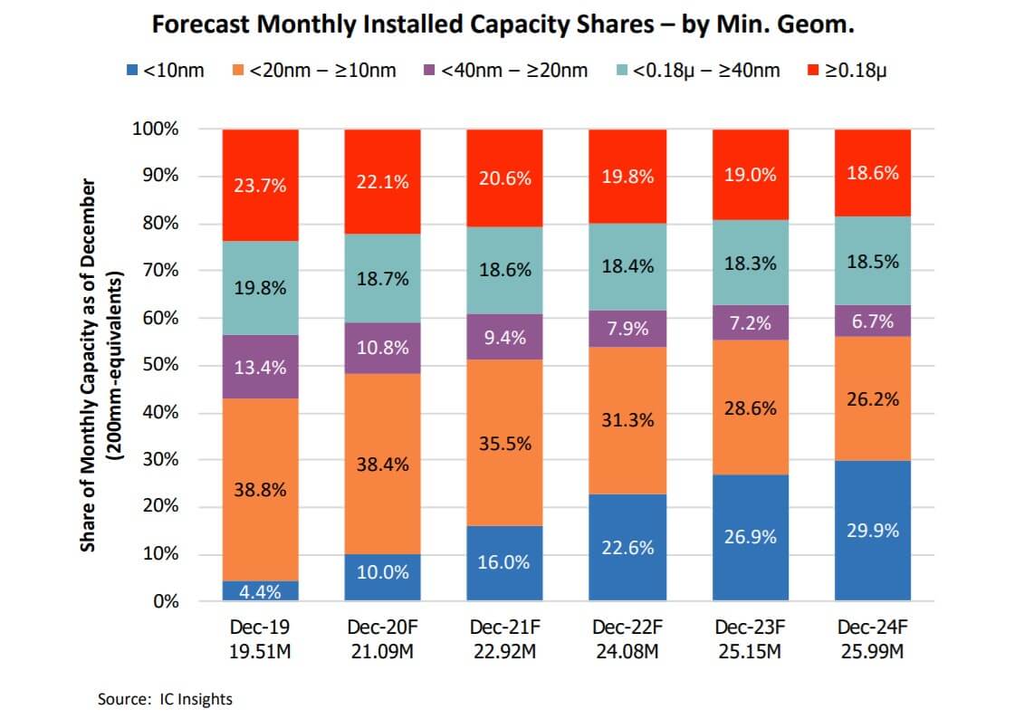
According to the latest report released by IC Insights yesterday, starting from 2024, IC production capacity with leading (<10nm) processes is expected to grow and will become the largest part of the industry's monthly installed capacity.
IC Insights pointed out that by the end of 2020, <10nm capacity is expected to account for 10% of the IC industry’s total wafer capacity, and then is forecast to rise above 20% for the first time in 2022, and increase to 30% of worldwide capacity in 2024. What constitutes a generation and how to measure the minimum process geometry gets more difficult every year. Therefore, any assumptions made regarding the wafer fab capacity of new process technologies can have a big impact on the forecast for wafer capacity by minimum feature size.
The report stated that there is tremendous motivation to continue shrinking minimum geometries because the benefits are many: higher speed, lower power consumption, lower cost per unit area, etc., but there comes a point where diminishing returns make chip designers question whether the high cost is worth it. The cost benefits of scaling aren’t what they used to be.
Equipment costs associated with <10nm process technologies have soared to the point where they have become prohibitive for many IC suppliers. Consequently, only Samsung, TSMC, and Intel currently operate fabs using <10nm process technology.
Meanwhile, design difficulties (for example, continuing to shrink DRAM and NAND flash memory cells) stand in the way of the scaling methods that the IC industry has used for many years. Challenges are also mounting for complex logic-based chips such as microprocessors, ASICs, FPGAs, and other advanced logic devices.
IC Insights believes the pace of migration of finer feature sizes for complex logic-based chips will continue slowing as chip designers find it increasingly difficult to justify the higher costs. For applications that greatly benefit from higher speeds, lower power consumption, etc, there will be healthy demand for the leading-edge finFET processes and beyond. The roll out of half-step generations or enhanced versions of existing processes is also contributing to more time passing between each new generation node.