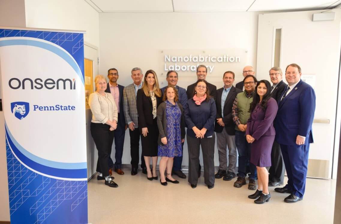
May. 17, 2023 /SemiMedia/ -- onsemi announces the signing of a Memorandum of Understanding (MOU) with Penn State University for an $8 million strategic collaboration that includes the establishment of the onsemi Silicon Carbide Crystal Center (SiC3) at Penn State's Materials Research Institute(MRI). According to the MOU, onsemi will fund SiC3 with $800k per year over the next 10 years.
In addition to conducting SiC research at SiC3, Penn State and onsemi will raise awareness about the increasing demand for tech jobs in the semiconductor industry. This is part of their efforts to enhance the share of U.S. semiconductor manufacturing. They also will partner on workforce development initiatives such as internship and cooperative programs and include SiC and wide bandgap crystal studies in Penn State’s curriculum. The relationship with Penn State is part of onsemi’s commitment to promoting STEAM (Science, Technology, Engineering, Arts, and Mathematics) education, ranging from helping K-12 students in underserved communities to university collaborations that support the development of the workforce for today and the future.
“onsemi is a proven innovator, delivering a comprehensive portfolio of intelligent power and sensing technologies to enable and accelerate sustainable solutions across multiple markets,” Weiss said. “At the same time, as per the National Science Foundation’s research expenditure rankings, Penn State is ranked first in materials science and second in materials engineering. We have world-class nanofab and characterization facilities that support research on thin films, silicon carbide and other materials used in semiconductors and other technologies. These complementary capabilities between onsemi and Penn State will have a strong impact on research and development, economic growth, and workforce development.”
Penn State’s capabilities make them an ideal academic partner for onsemi to advance the state of the art in silicon crystal growth.
“Penn State is uniquely positioned to rapidly establish a silicon carbide crystal growth research program,” said Pavel Freundlich, chief technology officer, Power Solutions Group, onsemi. “The university offers a wide breadth of capability based on its current materials research, wafer processing capabilities in its nanofab facility, and a comprehensive, world-class suite of metrology instrumentation.”
“Over the next decade, this collaboration will enable Penn State to become the nation’s leading resource for semiconductor crystal science and workforce development,” said Justin Schwartz, Penn State executive vice president and provost. “And this would not be possible without the relationship-building efforts of Priya Baboo, senior director of corporate and industry engagement, and the technical expertise of Joshua Robinson, professor of materials science and engineering, and their counterparts at onsemi.”
Scott Allen, vice president, University Relations, onsemi, added that “Penn State’s expansion of its curriculum to offer specialty courses in SiC and wideband gap technology will play a key role in meeting onsemi’s strategic workforce development goals and help to meet American semiconductor workforce goals as outlined in the recently signed CHIPS and Science Act.”


All Comments (0)