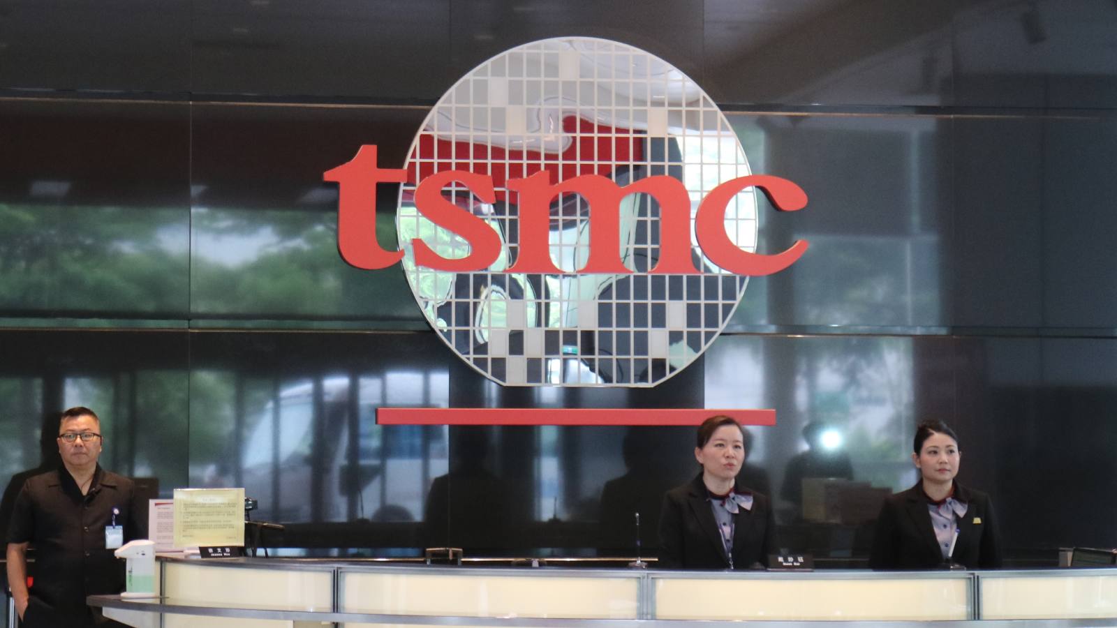
Recently, TSMC announced a 3nm process plan, with a planned investment of 19.4 billion US dollars. According to the plan, TSMC will start construction of the new factory in 2020 and complete equipment installation in 2021. It is expected to be put into operation as early as the end of 2022 to early 2023 and to employ 4,000 employees.
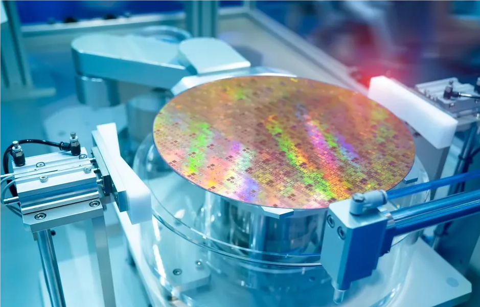
TSMC's 7nm process has been mass-produced this year. The first 7nm chip is the ASIC bitcoin chip. The chips used in this process include Apple A12, Hisilicon Kirin 980, AMD and NVIDIA's 7nm CPU/GPU chips. Compared to the 16nm FF process, TSMC's 7nm process (code N7) performance increased by 35%, energy consumption reduced by 65%, and triple the transistor density. At the beginning of 2019, the 7nm+ (code N7+) process of the EUV process will be introduced, and the transistor density will increase by 20%, and the power consumption will be reduced by 10%, but the performance will not change.
At the 5nm node, TSMC will invest $25 billion to develop the 5nm process. It is expected to start production in 2019 and mass production in 2020. Compared with the 7nm process, TSMC's 5nm process can reduce energy consumption by 20%, transistor density by 1.8 times, and performance is expected to increase by 15%. If new equipment is used, it may increase by 25%.
At the 3nm node, TSMC stated that it invested hundreds of engineers in early development last year. As announced recently, the factory will be built in Tainan, covering 28 hectares, close to TSMC's 5nm factory. 3nm technology can be said to be close to the physical limit of semiconductor technology, and it is currently in the laboratory stage, TSMC also admitted: "3nm process technology is difficult, it is a big challenge."


All Comments (0)